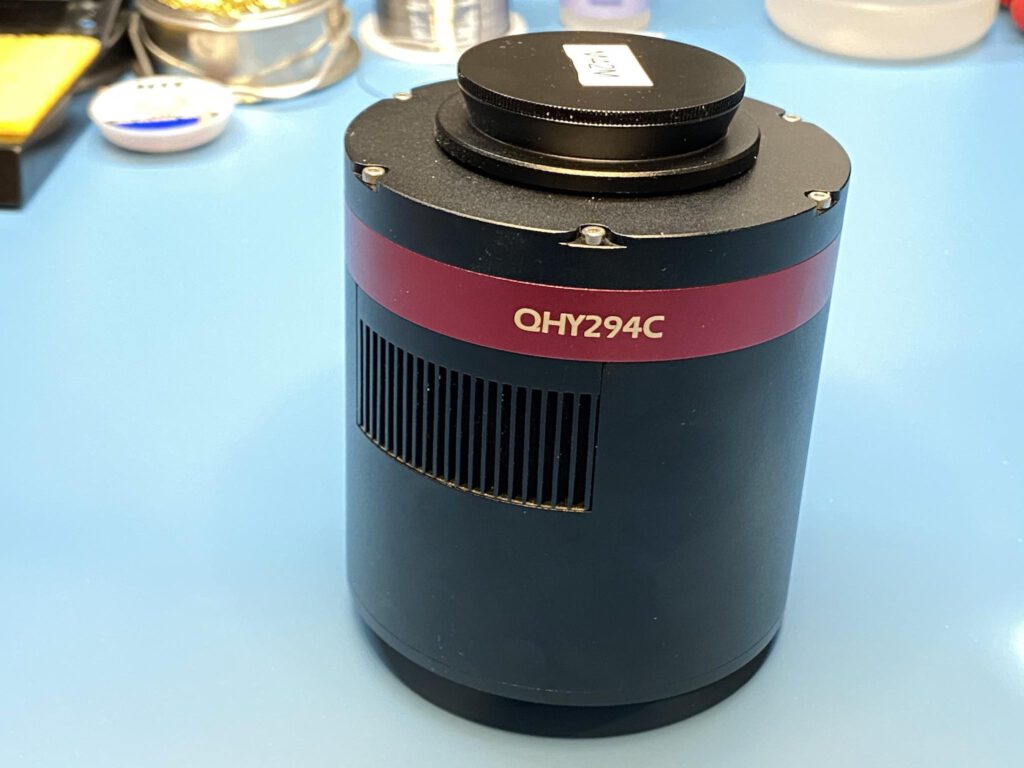
I bought a QHYCCD QHY294C in 2017 and have been using it on top of my main imaging rig as a secondary camera, as well as a test subject for the development of the native QHY driver in N.I.N.A. Its normal astrophotography configuration has it attached to a Canon EF 200mm f/2.8L II lens and an Astromechanics ASCOM focuser. The pixel scale of this setup, a hefty ~2.75 arcsec/pixel, was not very optimal. Although 200mm is what one can consider wide-field photography in the context of astrophotography, the 4.63um2 pixels of its Sony IMX294 4/3 format sensor left the finer details of objects being a bit too blocky (ie, undersampled) for my liking. Otherwise, it’s a fine sensor in a quality housing.
When QHY announced that they figured out how to unlock the Quad-Bayer superpixel of the IMX29/IMX492, I asked if a QHY294C could be converted to have the functionality of a QHT294C Pro. The ~1.37″/pixel scale of the unlocked 47MP mode would be far more pleasing compared to the existing 11MP resolution. This would mean being able to switch between two modes: 11MP with 4.63um2 (super)pixels, or “unlocked” at 47MP and 2.315um2 pixels. Dr. Qiu Hongyun, QHYCCD’s founder, said it was possible. The conversion would not be easy and would involve soldering, as the classic QHY294C camera was not designed with this alteration in mind.
Overview
The conversion process comprises of 5 major steps:
- Disassemble the rear portion of the camera to access the main logic board.
- Desolder a 0? SMD resistor to remove the write protection of the USB controller’s configuration EEPROM.
- Write a new USB Product ID (PID) code to the EEPROM to change its USB identity from that of a QHY294C to a QHY294C Pro.
- Reprogram the camera’s Xylinx Artix-7 FPGA via JTAG. This FPGA actually drives the sensor and is responsible for managing its main operating parameters.
- Replace the 0? EEPROM write-protect resistor and reassemble the camera.
This task was near my limit of experience as I’ve had minimal dealings with SMD rework and FPGA/CPLD programming. This project provided a good avenue to do and observe these things at a high level and become more comfortable.
Tools and supplies
- Proper anti-static measures in the work area. Namely, a grounded wrist strap and mat for the work area
- A quality soldering iron with fine tip, flux pen, and fine solder suitable for SMD work
- A magnifying task lamp or similar device
- Fine point or grasping electronics tweezers
- A Xylinx FPGA download cable
- An assortment of electronics project jumper cables
- IC test clips and some wire, or a 1×6 position 1.27mm pin pitch male header
- 99% isopropyl alcohol, cotton swab, and microfiber cloth for cleaning
Required software
- Cypress Semiconductor EZ-USB FX3 development suite
- Xylinx Vivado Lab Edition
Both pieces of software are free to download and use, but the companies do require you to make an account to do so.
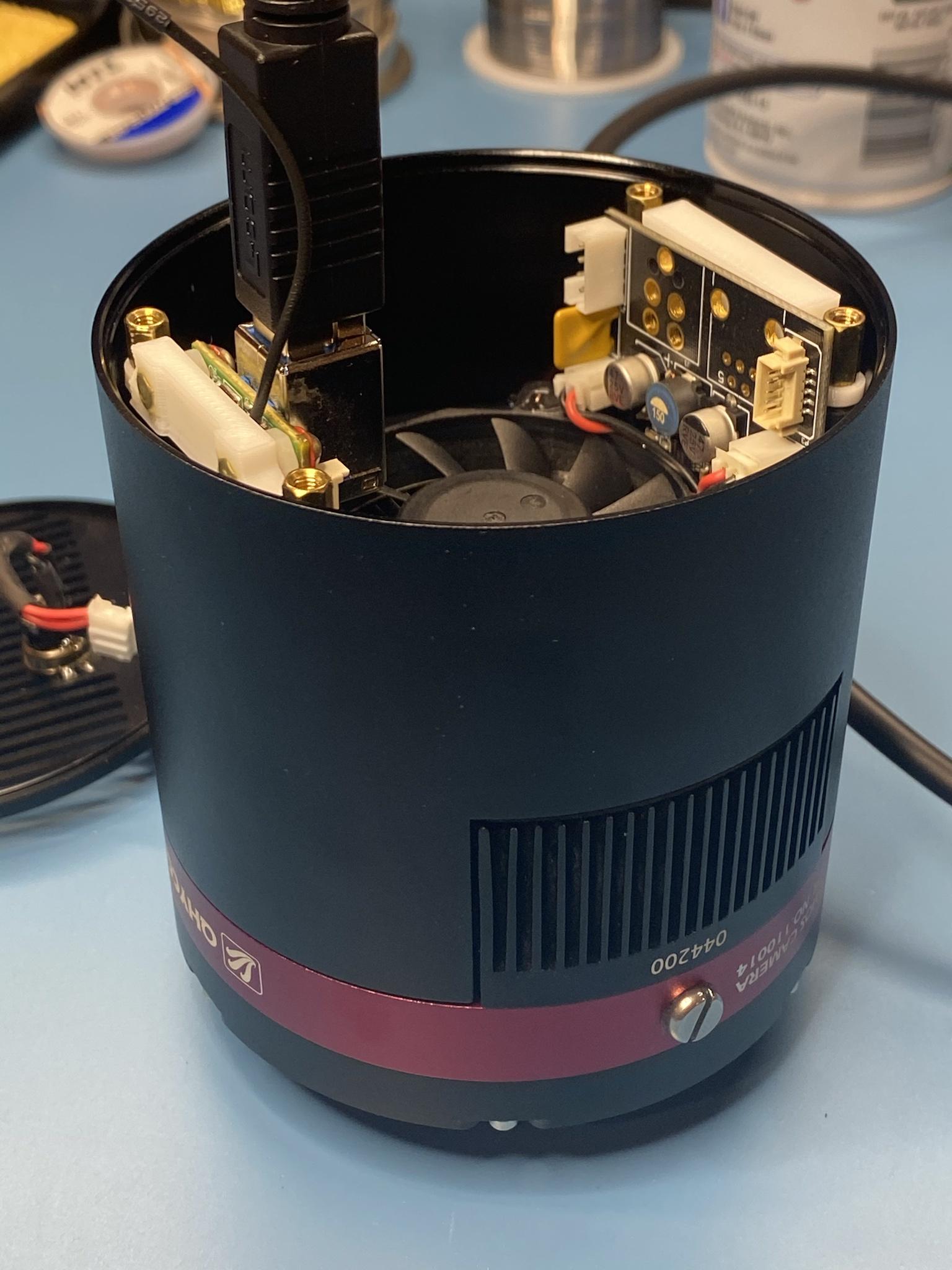
Initial disassembly
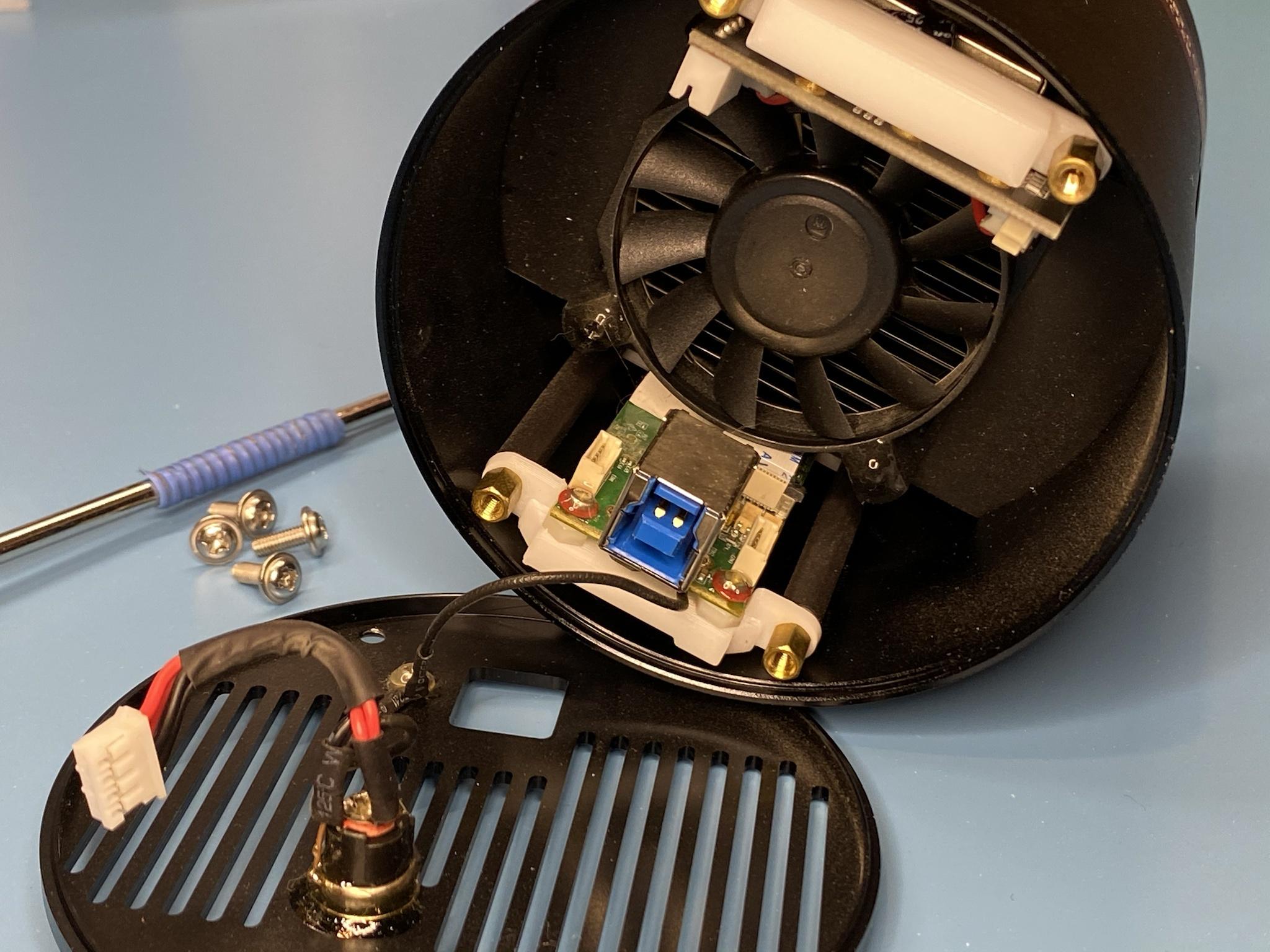
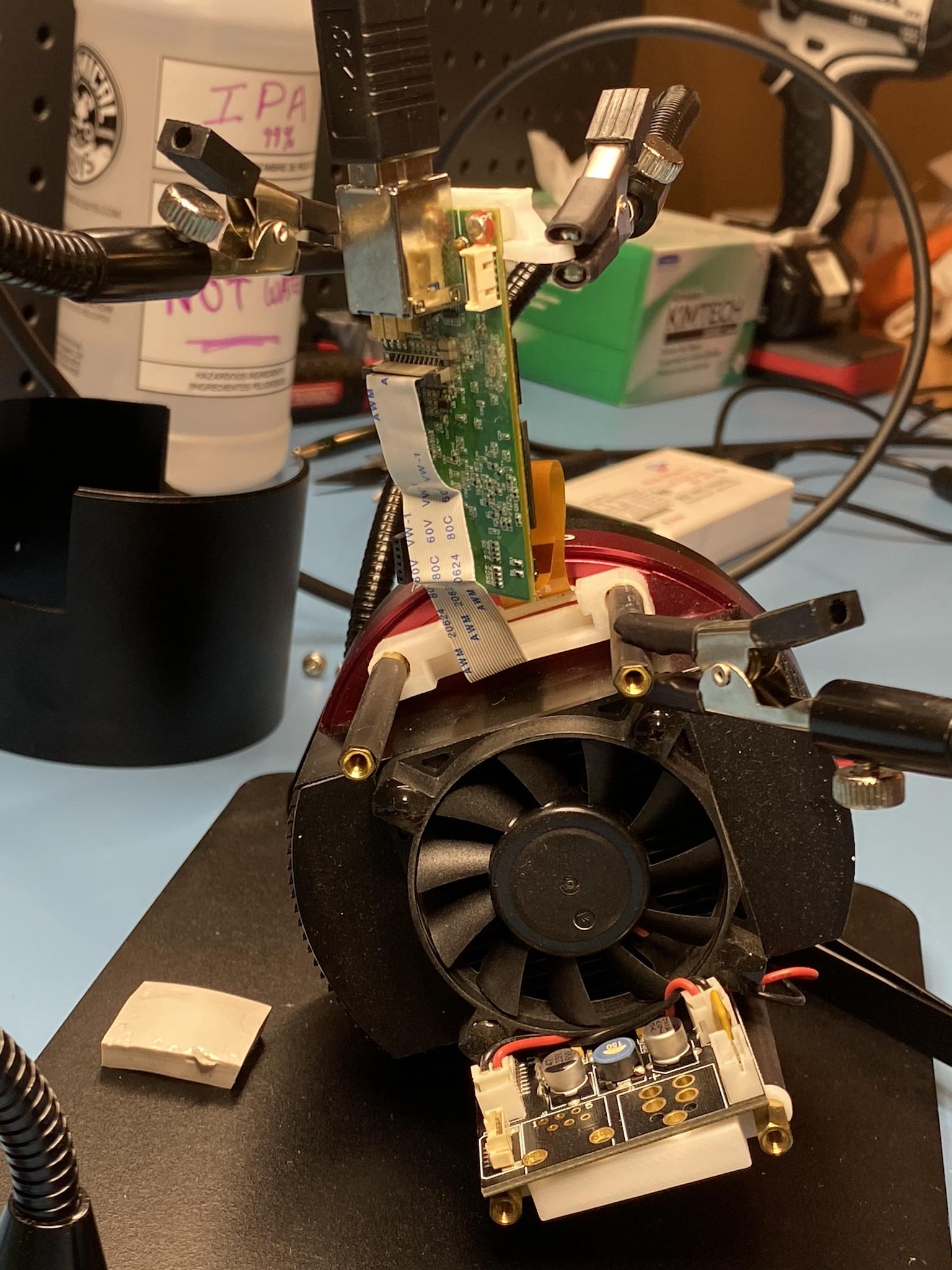
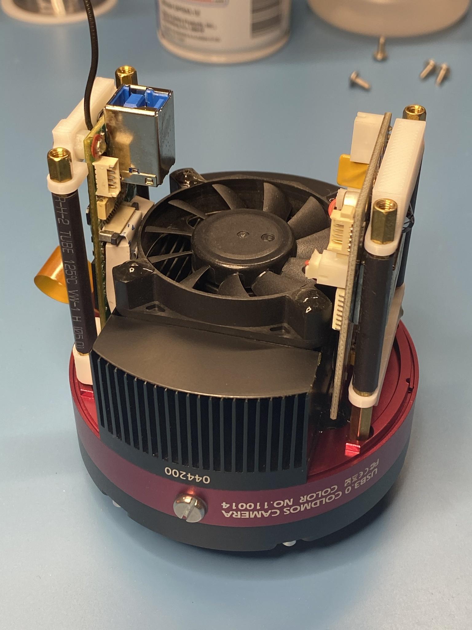
Removal of the four rear screws allows the rear faceplate plate to lift off. In this photo, we see the main board that has the camera’s core processors on the bottom, and the TEC controller board above it. The logic boards are affixed to white brackets and secured to the chassis with the brass standoffs. These standoffs also serve as anchors for the rear faceplate.
The 12V power input connects via mini Molex connector to the TEC board. A small ground wire connects a ground point on the faceplate to the main board.
We are only concerned with the main logic board, the board with the USB socket on it. The brass standoff screws must be removed and the ground wire disconnected from the faceplate. The screw that secures the black ground wire might be coated in a layer of adhesive. This adhesive can be picked off to access the screw head.
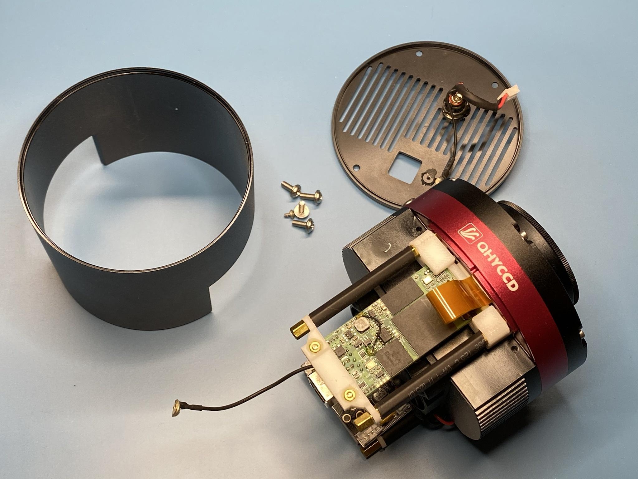
With the ground wire now removed, the main body can be set aside. Take care to avoid damaging the orange ribbon cable, seen in the above photo adjacent to the red trim ring.
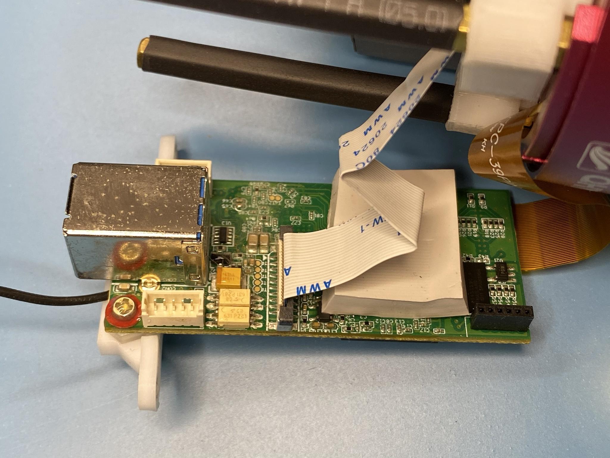
Removal of the two brass standoff screws allows the main logic board to be gently pulled out. It has two ribbon cables attached to it. The orange ribbon cable is secured to its connector with adhesive so I opted to avoid disturbing that. The white ribbon cable, seen in the above photo, may be removed by lifting the friction clamp on its connector which allows the cable to lift out. A foam block with silicone grease on its board-oriented side lays on the pcb, under the cable. This acts as a thermal barrier for the ribbon cable as the board’s main ICs are on the reverse side and they shed a non-trivial amount of heat while operating.
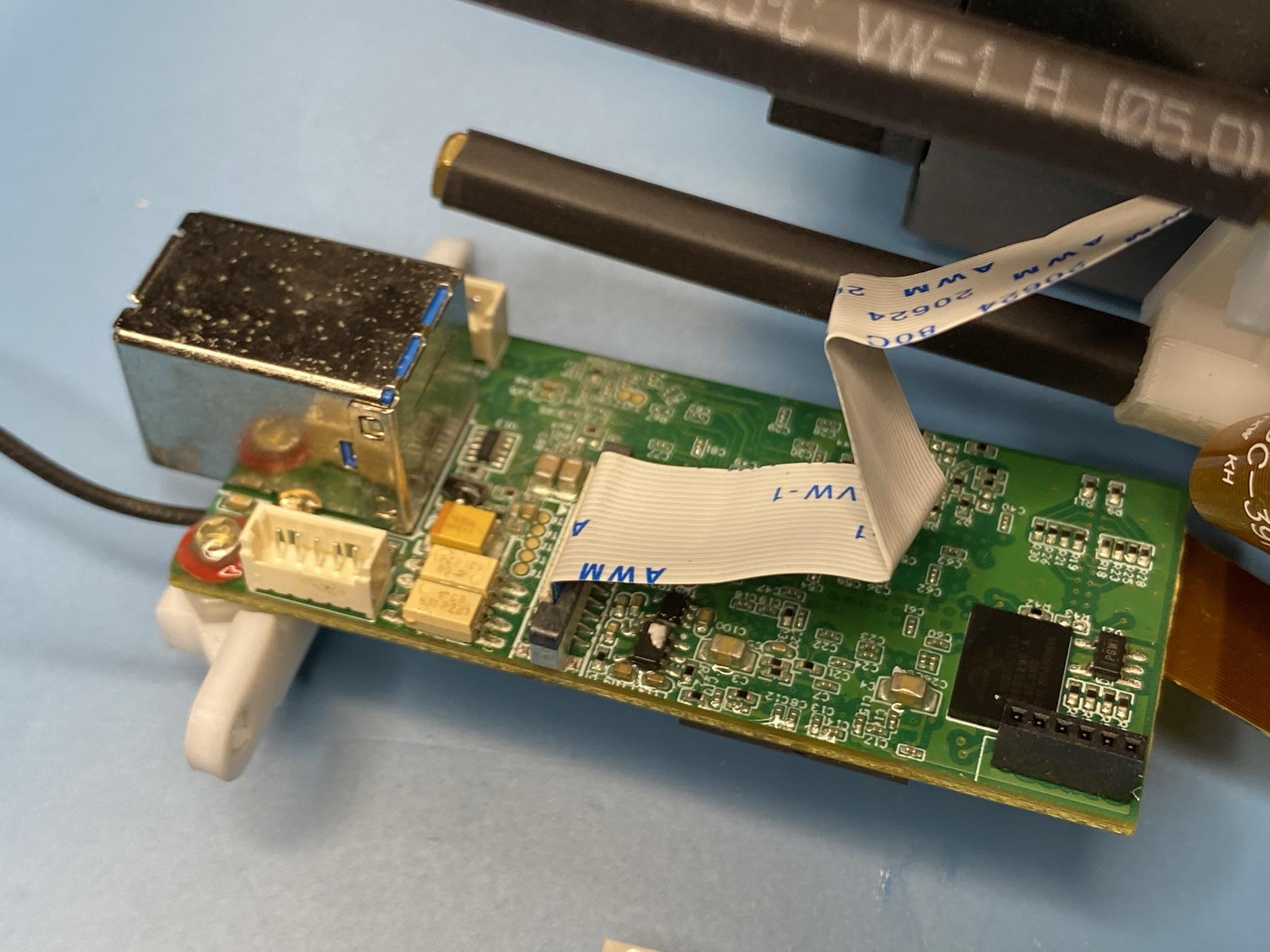
Main logic board, sans foam insulator. The black clip on the ribbon cable connector gently pulls up to release the ribbon cable.
Desoldering the write-protect resistor
Desoldering the USB EEPROM write-protect resistor is simple and should not pose any difficulty to those with minimal SMD experience. A fine point on the soldering iron and patience are all that’s needed. This 0? resistor is very small, only 1mm long. It is highly recommended to do this work under a magnifying task lamp or ocular.
The strategy is simple: gently grab the resistor with electronics tweezers in one hand and heat one end of the resistor with the point of the soldering iron with the other. Gently pull on the resistor as it is heated and, eventually, the solder will soften and the end will lift off the board. Swap hands and repeat for the other side, which will detach it entirely. Set it aside in a safe place.
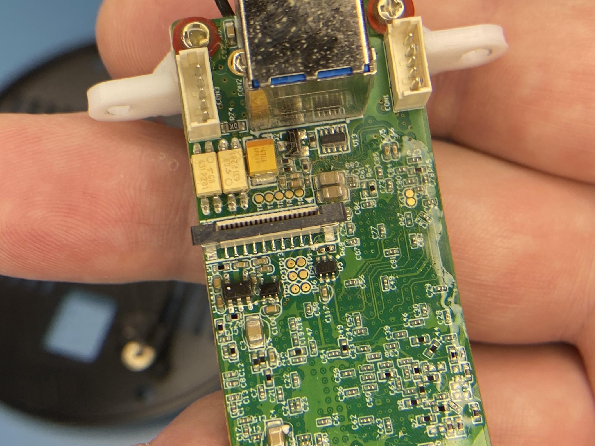
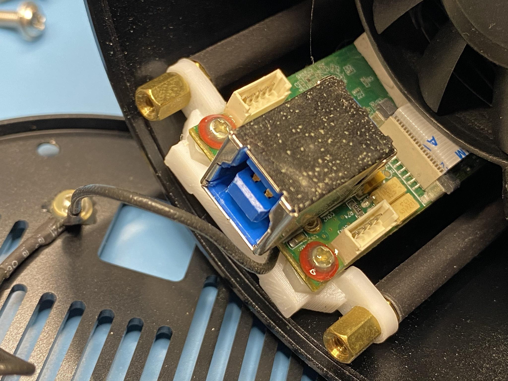
Resistor R68 is the component that must be removed. With the USB connector oriented to the top, R68 is located under the right side of the ribbon cable connector, between that and the EEPROM it protects.

Securing the logic board and the rest of the camera body is important in order to work comfortably. I use magnetic “helping hands”, with two clips to hold the board and one to keep the body from moving. The orange ribbon cable still connects the two, so care must be taken that it is not accidentally damaged by excessive pulling or kinking.
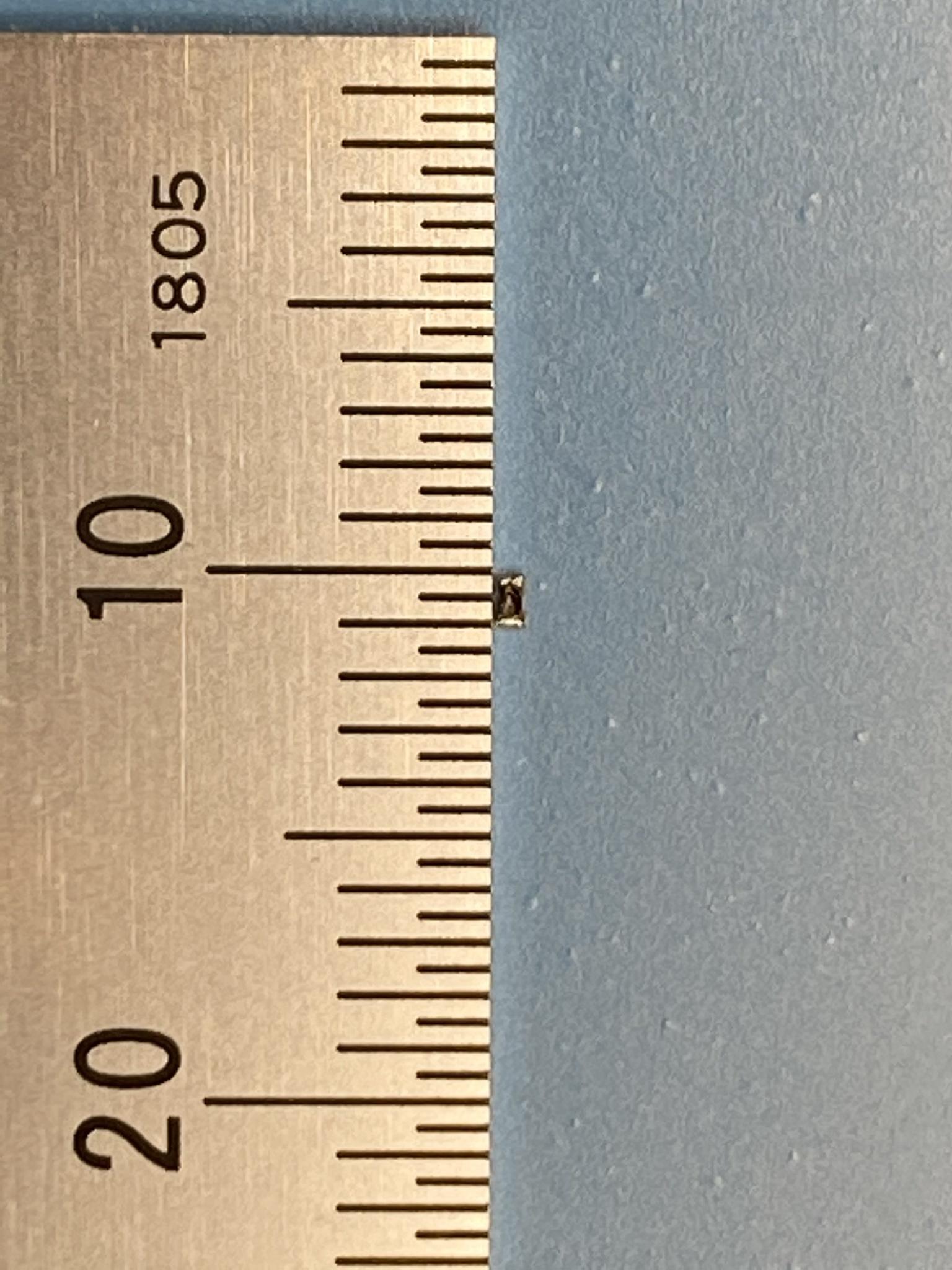
Once R68 is removed, put it in a safe place so that it can be reattached later. As you can see, it is quite small and can be easily mistaken for a piece of dust or debris.
Updating the USB PID
The USB Product ID code is a special identifier that all USB devices have and is part of the USB standard. It goes along with another code, the Vendor ID (VID). Together, they identify the Vendor and Product to the computer. This allows the appropriate USB driver to attach to the device, and for that driver to know how to properly operate the device. For QHY cameras, this allows the QHY USB driver to upload the model-specific firmware to the Cypress FX3 USB controller/GPIF on the main logic board. It also allows the QHY SDK to properly communicate with the camera.
Since the classic QHY294C will no longer be a QHY294C, we need to change the USB PID to that of the QHY294C Pro. We can do that now that we have removed the USB configuration EEPROM’s write-protect resistor.
The white ribbon cable that was unplugged to access R68 must be reinstalled. It facilitates power and data between from the TEC board and the main board, so the USB connection will not work without it. Insert it gently but fully into the connector and press down on the black retention latch to secure it. Make sure that it is not sitting askew relative to the connector it is in.
The main board is cumbersome to handle now because the two ribbon cables are short and don’t offer much slack. I used my helping hands to orient it in a vertical position so that I can plug my USB cable into it without putting stress on the ribbon cables. Another option is to reinstall the board into the body, but you will need to remove it again for the next step as installing the board back into the camera body will hide the JTAG header.

Reprogramming of the PID is done using the EZ-USB USB Control Center app. It is a very classic procedure, with reading from one register and writing to another. You can see the new PID code being entered and then read back in the above screenshot. That’s all there is to it.
Updating the Xylinx FPGA
Dr. Qiu furnished new FPGA code in the form of Xylinx bin and prm files. Uploading them to the FPGA will enable the pixel unlocking and other functions that are required for driving the sensor. Getting the new programming into the FPGA is tricky since it cannot be done over the USB connection. Instead, it is done via the JTAG header on the main board using a JTAG download adapter for Xylinx chips.
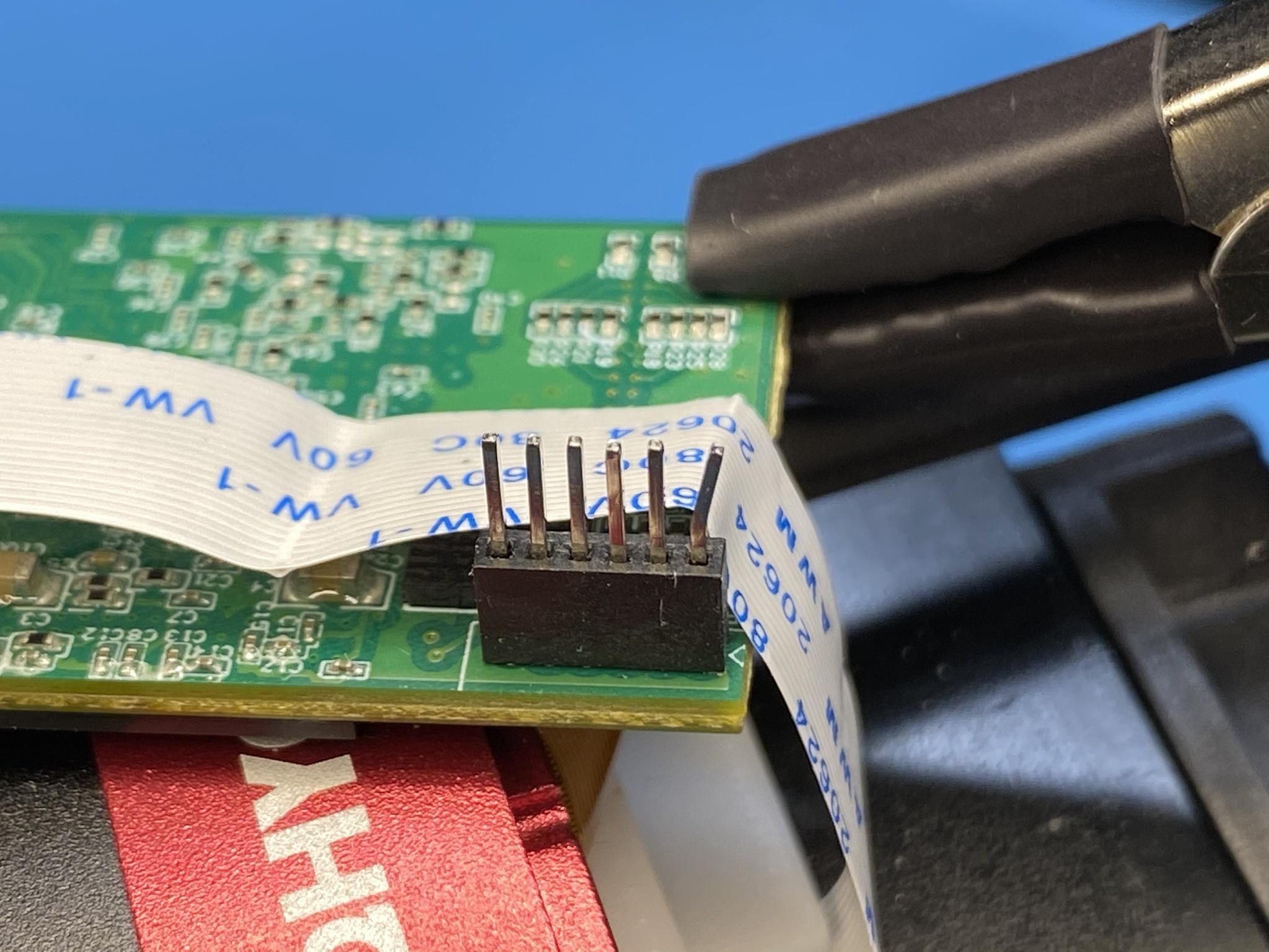
The above photo shows the 6-pin female header that serves as the JTAG connector. It has a 1.27mm pitch to the pins, and I didn’t have any of these on hand to use. I improvised by removing the pins from a 2.0mm pin pitch header and inserting them into the connector. My strategy was to use IC test clamps on each pin, then connect the clams to the Xylinx download cable.
The pinout is important, and the roles of the pins are not silkscreened onto the board. In the above photo, pin #1 is on the right, with the slightly bent pin inserted into it. The silkscreened caret index mark on the board at the base of the header appears to indicate this fact. The following JTAG pinout was found:
1: TMS
2: TDI
3: TDO
4: TCK
5: VREF
6: GND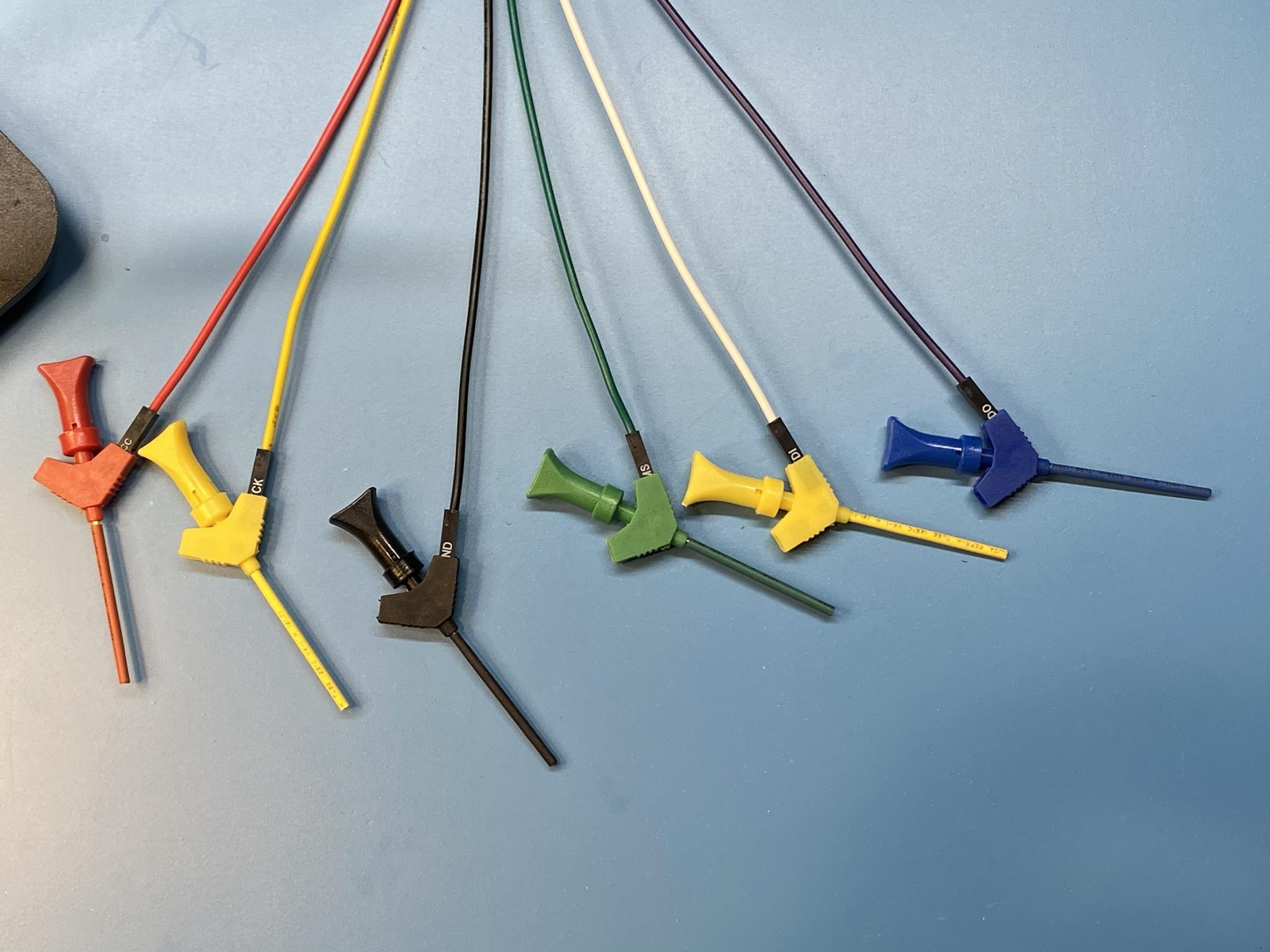
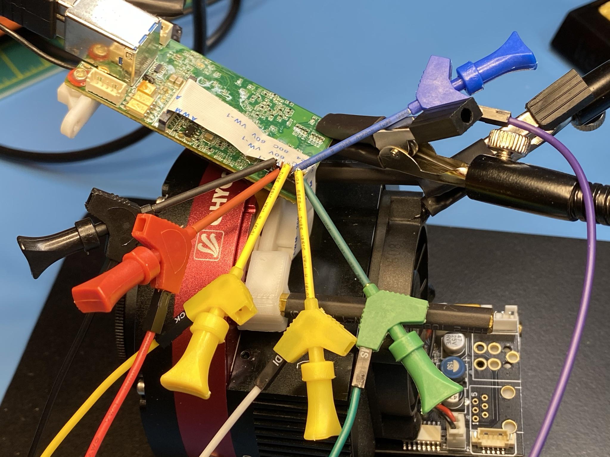

The above images show the JTAG wiring. I then applied power to the main board by plugging its USB port into my computer. It now had 2 connections to my PC: the regular USB, and the JTAG connection through the download cable. The JTAG wiring situation would have been a lot neater if I had some 1.27mm pin pitch headers on hand. I ordered some from Digi-Key, but they did not arrive by the time I wanted to move on with this project.
I then opened up Vivado’s Hardware Manager and connected to the board. Setting up the upload of the new FPGA programming and it actually uploading was about a 10 minute process, and it’s best to make sure that the board and the things connected to it are stable and won’t go anywhere. It’s a good time to take a break.
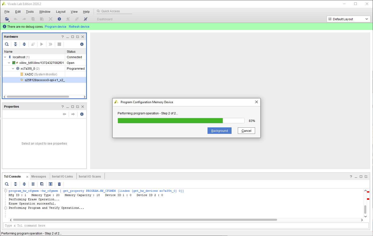
The view from Vivado during the upload process.
Finishing up
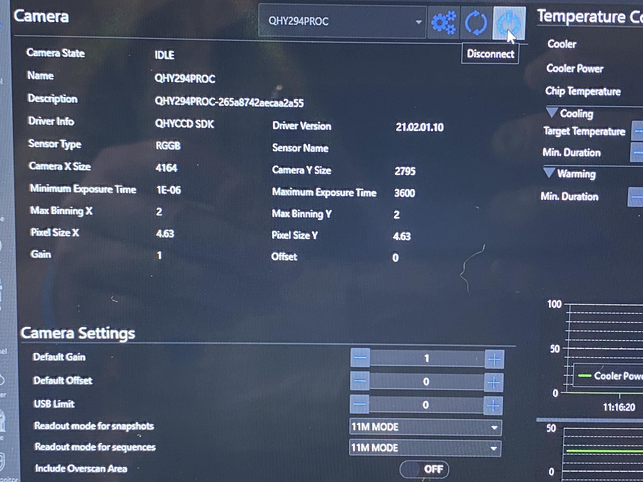
Close Vivado and remove all JTAG cabling. Unplug the main USB cable so that the board de-energizes. Then plug it back in and open the camera in N.I.N.A., SharpCap, or QHY’s own EZ_CAP app to see if you can connect to it.

Once you have verified that you don’t have an expensive brick sitting in front of you, you can start putting the unit back together.
Disconnect all external cabling and put the unit back together in the reverse order from which you disassembled it. Be sure to take extra care around two areas:
- The insulating foam block must be positioned with the greasy silicone side down against the logic board.
- Take extra care that the orange ribbon cable does not get pinched between the sleeve and the colored trim ring when sliding the body sleeve back on and seating it.
You can also take this time to clean out any dust if yours has seen some duty.
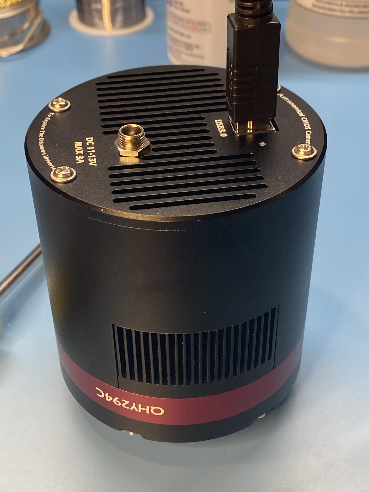
Reconnect the rear faceplate’s ground connections and plug the 12V DC feed back into its socket on the TEC board. Fasten down the rear faceplate with the 4 screws and test the camera again.
Hello,
I have the same camera and I would like to make this modification too.
Do you have the sources of the Xilinx a updater project?
Regards
I got the high-res unlocked by qhy a couple of years ago, at no cost, only to discover later that the high-res images cannot be debayered!!
Did you find a way to debayer your exposures?
I fear this announcement of qhy was just marketing, at least for color cameras. In mono you have really advantages.